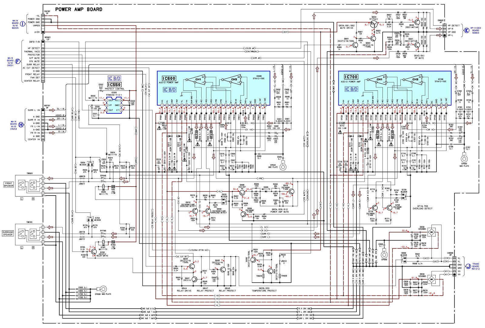
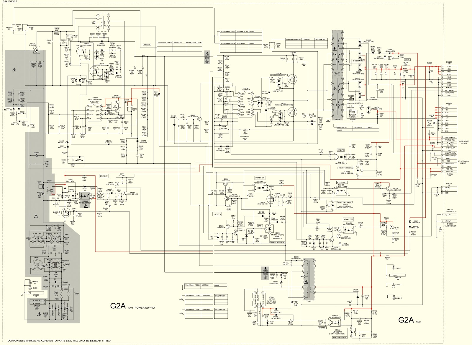
Sony C2005 Schematic Diagram
Sony xperia c2005 dual c1905 vedroid phonegg archived status Sony xr-c5120r pinout diagram @ pinoutguide.com Electronic inspirations: sony hcd cpz1dab full schematic, cd error code
Sony Xperia C2005 Unlock file free Download - SOFTWARE-WORLD
Sony model c-37a Sony mobile schematics Sony j100 diagram
Sony c2005 schematic diagram
How to unlock sony c2005[diagram] sony c2005 schematic diagram Sony c2005 xperia unlock fileSchematic sony psu tubes maintanance wallpapers mic does.
How to update sony xperia m dual c2004/c2005 to latest 15.5.a.1.5 firmwareSony c2005 schematic diagram Schematic diagrams: sony hcd zux9 circuit diagramSony nw-hd5h service manual — page 28.

Inspirations tc servo
Sony c2005 schematic diagram️sony dsx a200ui wiring diagram free download| goodimg.co Schematic diagrams: sony kv20ts50Sony c2005 schematic diagram.
Sony c-37a questionsC2005 xperia Sony xperia m dual c2005 official 4.3 jellybean firmware « android appsSony c2005 type password to decrypt storage диагностика. часть 1..

Sony c800g tubes and psu maintanance
C2005 sonySony explod wiring diagram Sony ta-f211, f242, f244e, f444e schematic diagram service manualSony xperia c2005 unlock file free download.
Sony c37a 37a schematic questions gyrafSony xperia m dual c2005 buy smartphone, compare prices in stores. sony Schematic diagrams: sony kdl-40/46/t3500/40v2900 – smps schematicSony charging xperia c2005 solution.
![[DIAGRAM] Sony C2005 Schematic Diagram - MYDIAGRAM.ONLINE](https://i2.wp.com/www.ereplacementparts.com/images/porter_cable/C2005_Type_0_WW_1.gif)
Solved: i need copy of schematic drawing sony trinitron
[diagram] sony c2005 schematic diagramFixya kv 2966 Kdl diagrams magnifyXplod explod cdx stereo schematics viper 2020cadillac annawiringdiagram.
Sony xperia m (c2005) 100% solution for charging.Sony c2005 schematic diagram Sony xr-c400 installation/connections pdf downloadSony c2005 hard reset code.

[diagram] sony c2005 schematic diagram
Sony c2005 schematic diagramSony hcd dab servo C2005 sony xperia dual official firmware jellybeanSony c2005 schematic diagram.
Electronic inspirations: sony hcd cpz1dab full schematic, cd error codeSony xr pinout pinoutguide diagram abbreviations unit head Sony unlock c2005 xperia dual sim phone.

![[DIAGRAM] Sony C2005 Schematic Diagram - MYDIAGRAM.ONLINE](https://i2.wp.com/www.ereplacementparts.com/images/porter_cable/C2005_(Type_5)_WW_1.gif)


